Intel Bets on Advanced Packaging to Pivot Toward AI Leadership
Inside the sprawling 200-acre campus of Intel’s Rio Rancho facility, a once-dormant factory known as Fab 9 has been revived. After sitting idle for over a decade—becoming a makeshift sanctuary for local wildlife—the facility has been transformed into the cornerstone of Intel’s high-stakes gamble: advanced chip packaging.
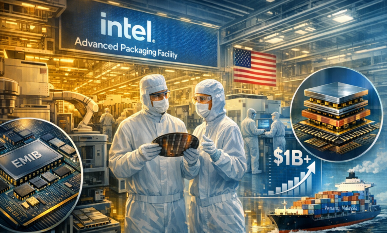
Backed by billions in internal investment and $500 million from the U.S. CHIPS Act, Intel is repositioning itself to capture the surging demand for Artificial Intelligence (AI) infrastructure. While the company has historically struggled to keep pace with Taiwan Semiconductor Manufacturing Corporation (TSMC) in raw wafer production, executives believe that “packaging”—the process of combining multiple smaller components (chiplets) into a single high-performance unit—will be the “very big differentiator” that restores the company’s former market dominance.
The Shift from Miniaturization to Integration
For decades, the semiconductor industry followed a predictable path of miniaturization. However, as the physical limits of shrinking transistors approach, the focus has shifted toward how these components are assembled. Advanced packaging allows for 3D stacking of processing units and high-bandwidth memory, squeezing more power out of the same surface area.
Intel’s Foundry arm is now going head-to-head with TSMC’s established CoWoS (chip on wafer on substrate) technology. Intel’s primary weapons in this fight include:
-
EMIB (Embedded Multi-die Interconnect Bridge): A process that uses microscopic “bridges” to connect components, reducing space and power consumption.
-
Foveros: A sophisticated die-stacking technology that enables 3D integration.
-
EMIB-T: The latest iteration, slated for rollout this year, which promises surgical precision in power efficiency and signal integrity.
Pursuing the Hyperscalers
Intel’s success hinges on securing “foundry” customers—tech giants like Google and Amazon that design their own custom silicon but require specialized facilities to assemble them. Sources suggest Intel is in ongoing discussions with both companies.
The financial implications are significant. Intel CFO Dave Zinsner recently revised packaging revenue projections from hundreds of millions to “well north of $1 billion,” noting that packaging deals could generate revenue even before the company sees meaningful returns from its traditional wafer business. To accommodate this growth, Intel is also accelerating its footprint in Malaysia, building additional assembly and test capacity in Penang to meet “rising global demand.”
A Cultural and Strategic Pivot
The most profound change within Intel may be its new “open” business model. Historically, Intel only packaged its own proprietary chips. Today, the company allows customers to “enter and exit the highway” at any point in the manufacturing process. A client can now bring wafers produced elsewhere to Intel specifically for its advanced packaging expertise.
Despite the technical prowess, market dynamics remain a hurdle. Analysts suggest potential customers may be cautious, fearing that shifting business to Intel could jeopardize their supply allocations with TSMC.
The “System-in-Package” Era
Intel’s strategic pivot to advanced packaging represents a pragmatic acknowledgment of the current semiconductor landscape. By decoupling packaging from wafer fabrication, Intel is creating a lower barrier to entry for “hyperscalers” (Google, AWS, Meta) who are desperate for AI-capable silicon but are currently bottlenecked by TSMC’s capacity limits.
Industry Impact: If Intel successfully scales EMIB-T, it could effectively break the TSMC monopoly on high-end AI accelerators. From a technical standpoint, Intel’s packaging-first approach acts as a “Trojan Horse”; once a customer trusts Intel with the “back-end” assembly, the transition to using Intel’s “front-end” wafer fabrication becomes a much smaller leap. However, the true metric of success will be Capital Expenditure (CapEx). As Foundry head Naga Chandrasekaran noted, the market should watch for a surge in Intel’s spending—this will be the definitive signal that multi-billion dollar contracts have moved from the negotiation table to the factory floor.